

Recently, the active matrix EWOD (AM-EWOD) jointly developed by ACXEL, LINKZILL, and other institutions was successfully published as an important research result at the IEDM conference, a top conference in the field of microelectronics. This chip achieves extremely high pixel density based on the minimal circuit design, realizing on-chip high-throughput, parallel processing of multi-channel biological samples, and the sample processing is sealed and independent of each channel, effectively avoiding cross-contamination. The density, uniformity, and stability of the micro-droplets generated on this chip are at the state of the art, which symbolizes that the research of active digital microfluidic chips has entered a new stage.
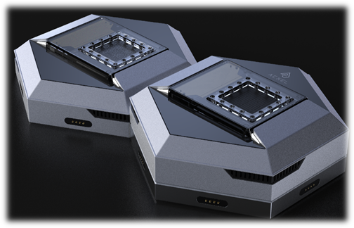
Figure 1. Active digital microfluidic platform
The main idea of microfluidic technology is to obtain a maximum output with minimal consumption, and all required information can be obtained with minimal sample collection. Specifically, microfluidics aims at the smallest reaction system (pico-liter or nano-liter), consumes minimum reagents and samples, and runs parallel independent reactions as more as possible, meanwhile keeping the isolation of the reaction system, reducing pollution, etc. As the manipulation object of microfluidic technology, microfluidics can cover a wide range of biological samples such as blood, urine, saliva, etc. Therefore, it has gradually developed into a key technology for point-of-care testing (POCT) in the field of in-vitro diagnostics (IVD).

Figure 2. Traditional in vitro diagnostics consume a lot of biological samples
The digital microfluidic chip is the main branch of microfluidic technology and has the highest application potential. The control of microfluidics is based on the principle of Electrowetting on Dielectric (EWOD): when there is liquid on the electrode, and a potential is applied to the electrode, the wettability of the solid-liquid interface at the corresponding position of the electrode can be changed, and the contact angle of the droplet-electrode interface changes accordingly. If there is a potential difference between the electrodes in the droplet area, a lateral driving force will be generated because of the contact angle difference, causing the droplet to move laterally on the electrode substrate. If we control the peripheral circuit and input the modulated voltage signal to the electrode array, we can control the droplets to be distributed and moved arbitrarily on the two-dimensional plane of the microfluidic chip.
The high pixel array determines the high-throughput processing of biological samples. In another word, a digital microfluidic chip with a large-scale pixel array is a prerequisite for realizing on-chip high-throughput, automated processing of biological samples. However, most traditional digital microfluidic chips currently use passive electrode arrays, of which each pixel electrode is directly connected to the control circuit through a separate wire. Increasing the number of pixels requires a huge number of signal lines and a more complex control circuit, which will undoubtedly and significantly increase the difficulty of array design and manufacturing. The poor array scalability has become a huge obstacle to the further development of this technology.
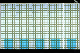
Figure 3. Freely controllable movement of the droplet
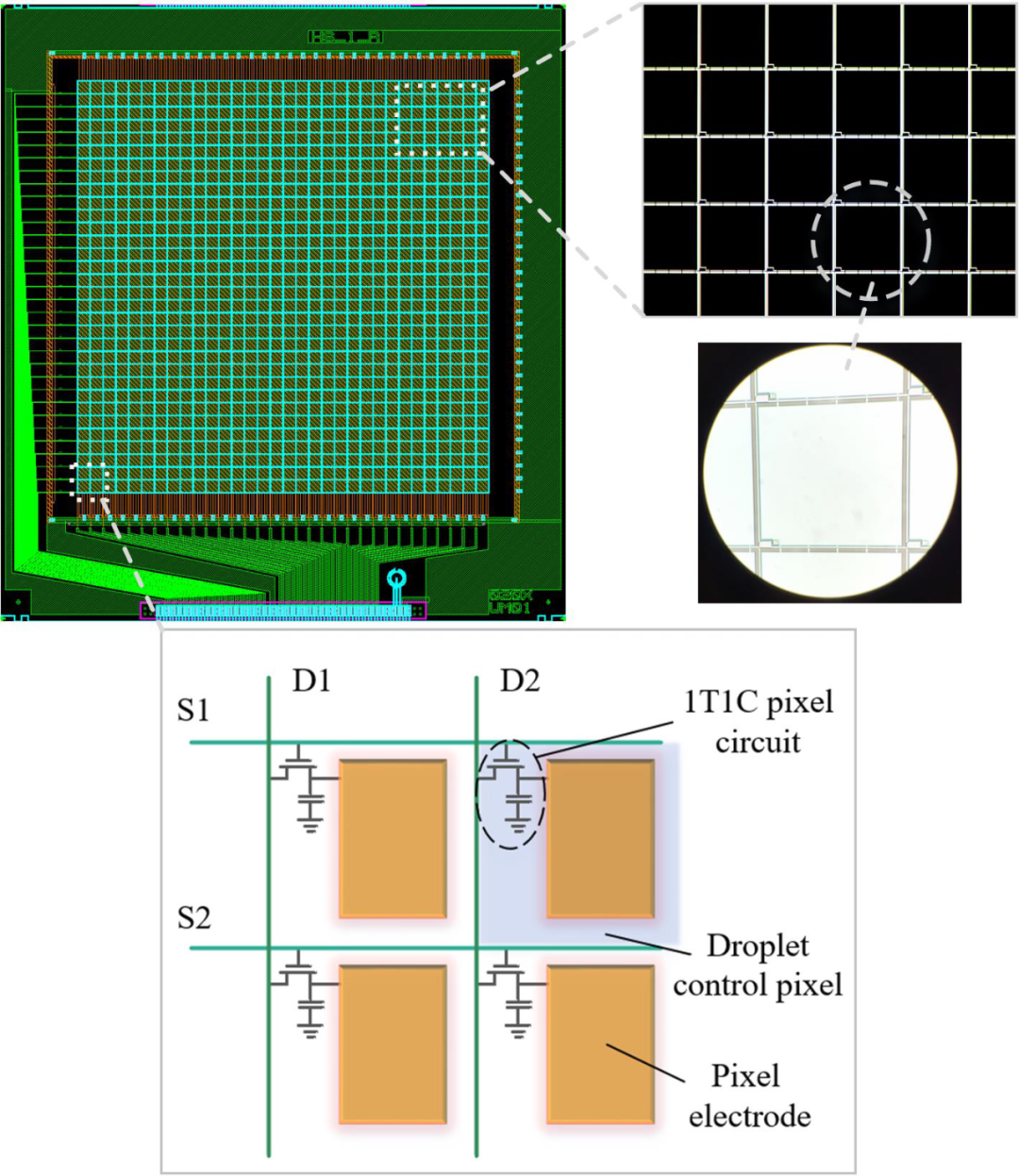
Traditionally, the number of pixels and the complexity of the control circuit seem to be of irreconcilable contradiction, but a new type of circuit can solve it by a clever design. One of the innovative routes is active matrix technology. The so-called active matrix technology is to integrate thin film transistors (TFT) into each pixel electrode. Each TFT is equivalent to an electronic switch, which includes a gate (G), a source (S), and a drain (D). Applying voltage to the gate can control the ON and OFF state of the connection between the source and drain electrodes. As shown in Figure 4, the gate of the transistor is connected to the row signals, the drain is connected to the column signals, and the source is connected to the pixel electrode. When a row signal applies a pulse voltage to the gate, the TFT switch of the corresponding row will be turned on. The column signal is then delivered to the pixel electrodes, and at this time, the corresponding driving voltage were "written" to each pixel electrode. Through this driving method of row and column scanning, an N (row)×M (column) array demand only N+M signal lines to independently control each of the pixels in the array. Compared with the passive array, the active matrix greatly reduces the number of signal lines and simplifies the structure of the control circuit. Theoretically, the application of active matrix technology to digital microfluidic chips has shown unique privilege of solving the problems in array scalability. However, in practice, due to the difficulty of interdisciplinary technology integration, few achivements that apply the active matrix technology to microfluidic chips has been reported so far.
Led by the teams from SIBET,CAS, ACXEL, LINKZILL, Cambridge University, and Shanghai Jiaotong University, a active matrix digital microfluidic chip (AM-EWOD) and supporting system based on thin film electronic active backplane technology have been successfully developed. This work provides the possibility to realize the entire process of large-scale, high-throughput digital biological experiments on a chip. The work were presented at the recently closed 2020 International Electronic Devices Meeting ,titled as "Large-area manufacturable active matrix digital microfluidics platform for high-throughput biosample handling".
In this research, the active digital microfluidic chip can digitally and parallelly process a variety of biological samples. It ensures the sealing of the sample and the independence of each channel while increasing the throughput, avoiding cross-contamination effectively. The team applied commonly used active matrix (AM) technology in flat panel displays to the digital microfluidic chips, integrating 32×32 pixels in an effective area of 10 cm2, so that the amount of pixels integrated on the chip increased exponentially, meanwhile, the single-pixel level micro-droplet manipulation has been realized. The droplets generated by this digital microfluidic platform have a high degree of uniformity, and their volume change coefficient is only 1%. Compared with the optimal performance of other microfluidic chips reported (9-pixel resolution and 4% change rate), the index has been significantly improved. Single-pixel-level droplet manipulation can greatly increase the utilization rate of array pixels, and improve the droplet control accuracy and sample processing throughput. The manufacturing of the active array backplane for this project was undertaken by Tianma Microelectronics through the multi-project glass (MPG) project.
With the concept of Active·Creative·Effective, ACXEL is committed to developing an intelligent digital microfluidic platform to achieve efficient sorting and precise enrichment of single cells, improve the efficiency of cell-related experiments, and shorten the research development period. The company's core technology is the development and system integration of electrowetting digital microfluidic chips based on large-area thin-film electronics manufacturing processes and apply it in single-cell omics research. Application fields include digital cell sorting, on-chip culture, drug screening, etc.
LinkZill is founded in Jan. of 2019 in Wuhan, and relocates the headquarter to Hangzhou in Jan. of 2020, then starts the R&D center in Shanghai since 2021. LinkZill's core value is "leading the technology–领, be dedicated and honest from the beginning to the end–挚". LinkZill is devoting to making technology serve people in a better and more efficient way.
LinkZill's core products are thin-film transistor (TFT) semiconductor chips (including corresponding functional materials and portable test/drive systems), with the applications of high-throughput DNA synthesis, active-matrix digital microfluidics, biochemical / photoelectric sensor and cutting-edge scientific research.
The IEEE International Electronic Device Conference is a top conference in the field of microelectronic devices with a history of more than 60 years. It enjoys a high academic status and extensive influence in the international semiconductor technology community. It is known by foreign media as the "Olympic in the field of microelectronic devices ". The conference mainly reports the latest research progress in international semiconductor technology, and is one of the main platforms for famous universities, R&D institutions and companies such as Intel and IBM to report their latest research results and technological breakthroughs. In recent years, many major technological breakthroughs in the field of integrated circuit technology have been officially announced through this conference.